
- JMY901
- JMY980
Série ARM9
JMY980

-
Description
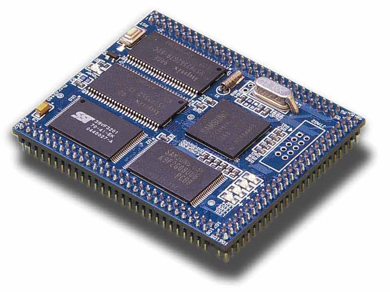
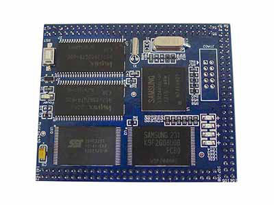
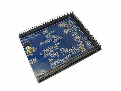
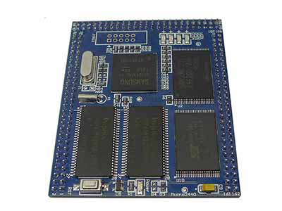
JMY980 is a core board, 6 layer board design, and
the use of same long wiring to meet signal integrity. It contains the basic 5V power supply
power circuit, JATG the debug port, the user debug indicator, reset circuit, as well as the
core of the CPU and the memory cell. FLASH memory cell contains the NAND Flash and NORFlash
two types, selectable via jumper J1 NAND or NOR boot the system. NOR Flash which put the
BIOS does not change often, NAND Flash programming complete system program (Bootloader,
kernel, file system, etc.).
-
Caractéristiques
- • Fréquence de fonctionnement: 400MHz
- • Interface: GPIO(56Pin, 2.0mm Spacing) interface PA: 1; LCD(50Pin, 2.0mm Spacing) and CMOS CAMERA interface PB: 1; System Bus Interface PC(56Pin, 2.0mm Spacing): 1; JTAG interface(10Pin, 2.0mm Spacing): 1
- • Alimentation: DC5V
- • Consommation d'énergie: 690mA
- • Dimensions: 63mm × 52mm × 10mm
- • Poids: about 20g
- • Température de fonctionnement: -40 ~ +85 ℃
- • Température de stockage: -65 ~ +150 ℃
| Operation Instruction | |
| Modèle N° | JMY980 |
| Interface | U-shaped interface(PA, PB, PC) |
| MCU | S3C2440A(Kernel: ARM920T) |
| SDRAM | 64M SDRAM; 32bit Data bus; Clock fréquence: Max.166MHz |
| Flash Memory | 2M Nor Flash and 64M Nand Flash |
| Data storage | 4096K bytes, 512 bytes/block |
| Display | 4 LED lights in the board (external TFT LCD screen) |
| Buzzer | No(PWM external) |
| System clock and RTC | Internal real-time clock (with battery backup),12M Passive crystal |
| Operating system | Linux2.6.X, WindowsCE5.0/6.0, uCos |
Produits Associés
-

MIFARE 1K (S50) -

MIFARE 4K (S70) -

MIFARE DESFire -
JMY6011 -
JMY6281 -
JMY6804 -
MR800 -
MR791 -
MR7911